ZAM (Z-Angle Memory)
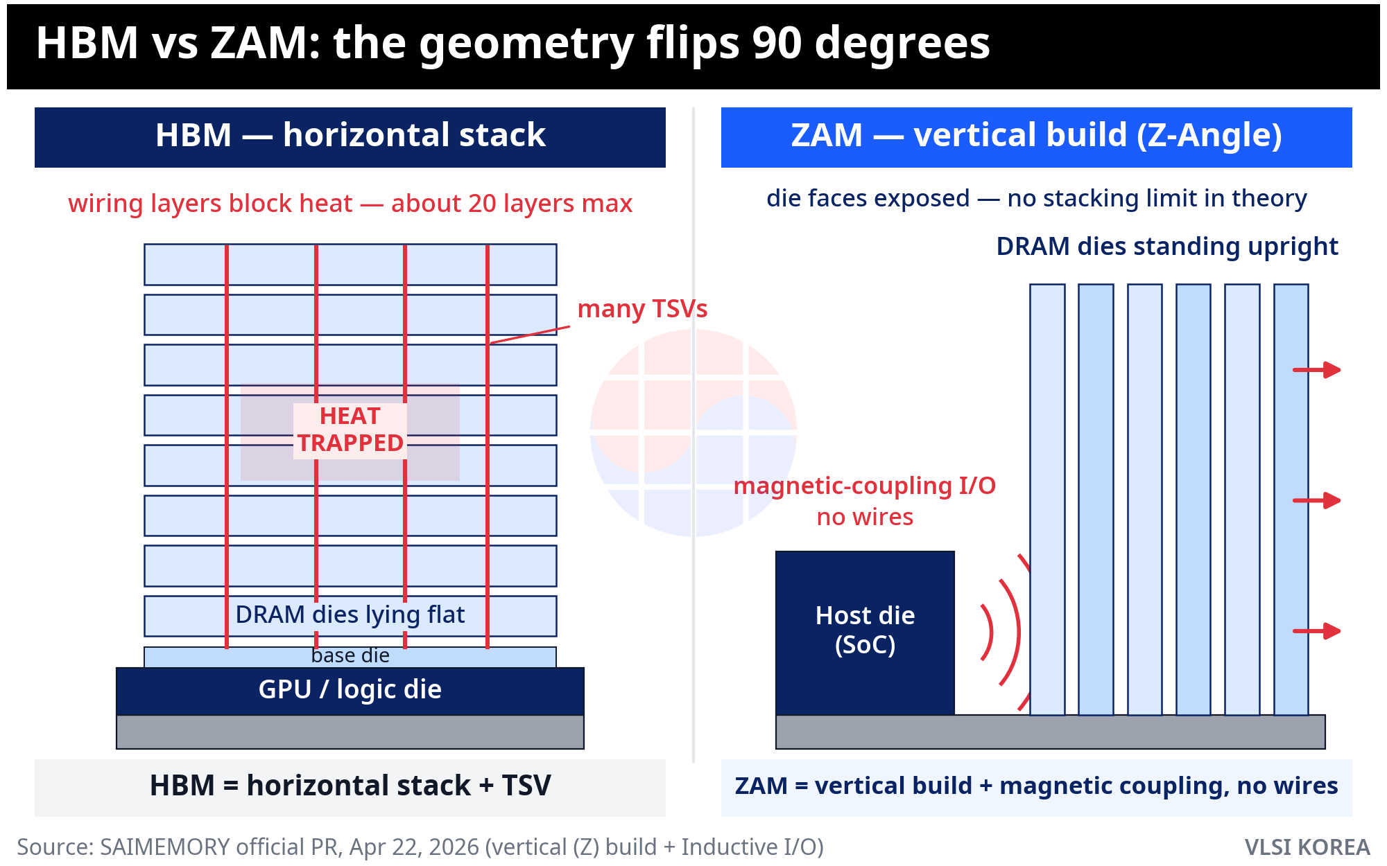
ZAM (Z-Angle Memory) is a next-generation DRAM-based memory technology that SAIMEMORY of Japan is developing toward commercialization together with Intel. Unlike high bandwidth memory (HBM), which stacks DRAM dies horizontally, ZAM stands the dies upright side by side — a “vertical build (Z-Angle)” — and connects them to the host die with magnetic-coupling wireless I/O instead of physical wiring.
Structure
In the vertical build, DRAM dies stand upright on the substrate rather than lying flat. Because the broad face of each die is exposed, heat is no longer trapped inside the stack, which SAIMEMORY states removes in theory the stacking limit of about 20 layers that wiring layers impose on HBM heat dissipation. The host die is connected through magnetic (inductive) coupling I/O with no physical wires.
Underlying technology — Intel NGDB
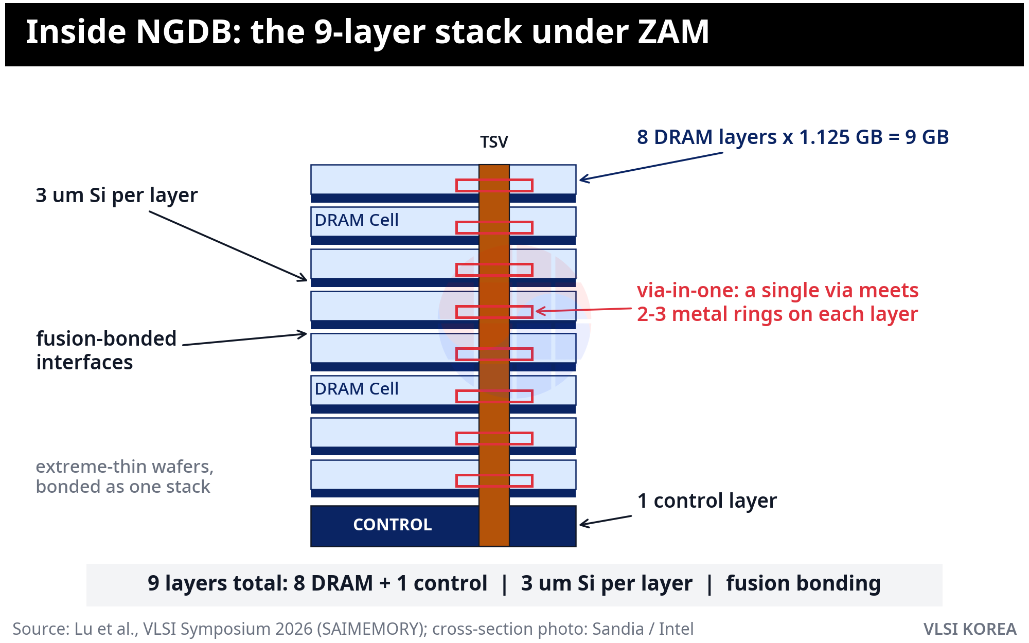
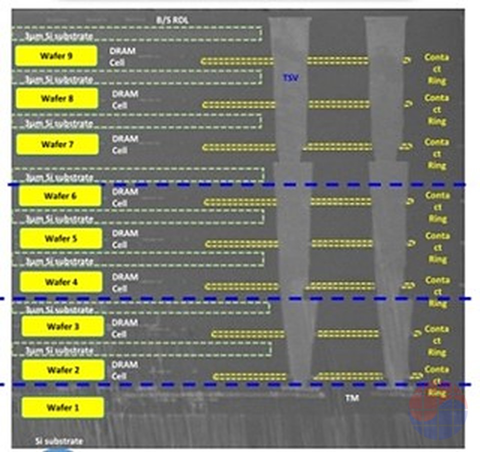
ZAM's bonding foundation is Intel's Next Generation DRAM Bonding (NGDB) initiative, carried out under the U.S. Department of Energy / NNSA Advanced Memory Technology (AMT) program with Sandia, Lawrence Livermore and Los Alamos national laboratories. A 2026 VLSI Symposium paper (Lu et al., SAIMEMORY) reports a nine-layer stack (eight DRAM layers of 1.125GB = 9GB plus one control layer), 3µm of silicon per layer, a single via-in-one meeting two to three metal rings per layer, and fusion bonding.
Comparison with HBM
| Aspect | HBM | ZAM |
|---|---|---|
| Die arrangement | Horizontal stack (dies lying flat) | Vertical build (dies standing upright) |
| Interconnect | Physical TSV wiring | Magnetic-coupling wireless I/O, no wires |
| Stacking limit | About 20 layers, limited by heat in wiring layers | Aims to remove the stacking limit in theory |
| Status | In mass production for AI data centers | Prototype targeted FY2027, commercialization FY2029 |
Timeline
| Dec 2024 | SAIMEMORY founded (wholly owned SoftBank subsidiary, Tokyo) |
| Feb 2026 | Collaboration agreement with Intel signed |
| Apr 2026 | Selected for a NEDO R&D grant program; Series A funding |
| Sep 2026 | MOU with SHINKO Electric Industries on packaging and manufacturing technology |
| Oct 2026 | Design and engineering engagement with SkyeChip |
| FY2027 (target) | Prototype |
| FY2029 (target) | Commercialization |
Related terms
HBM (High Bandwidth Memory) · DRAM · TSV (Through-Silicon Via) · Hybrid bonding · SAIMEMORY
References
- SAIMEMORY Corp., “SAIMEMORY and Intel Collaborate to Commercialize Next-generation Memory Technology”, Press Release, Feb 3, 2026.
- SAIMEMORY Corp., NEDO grant selection and Series A announcement, Apr 22, 2026 (vertical (Z) build + Inductive I/O).
- C.-L. Lu et al. (SAIMEMORY), “Multiple-Wafer (9-layer), Extreme thin (3µm-Si per stack) and Innovative Fusion-bonded Via-in-one Architecture for High Bandwidth 3D Memory”, VLSI Symposium 2026.
- Sandia National Laboratories, “From early R&D to mature technology” (NGDB cross-section photo, provided by Intel).
- HPCwire, “New Details Emerge on ZAM, the HBM Killer”, May 4, 2026.
- SAIMEMORY Corp., MOU with SHINKO Electric Industries, Sep 28, 2026.